
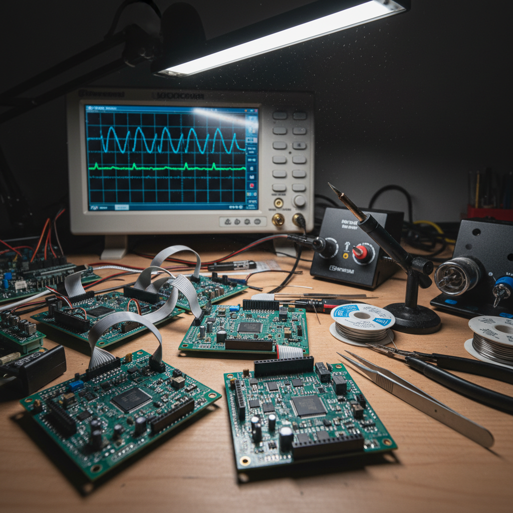
Hardware prototyping for startup CTOs racing toward demo day, engineers compressing revision cycles, and crowdfunding creators who need a working unit — not a render.
48h
PCB Turnaround
4-layer standard
0.1mm
Trace Width Min
Production-grade
500+
Prototypes Shipped
Since 2019
97%
First-Pass Yield
SMD assembly
We catch the problem before the board goes to fab.
Your schematic hits our bench and a hardware engineer — not an automated tool — walks every net, checks component footprints against your BOM, and flags DFM issues that would have cost you a respin. Most reviews complete in 4 hours.
- ▸Net-by-net schematic review against IPC-7711 and IPC-2221 design rules
- ▸Footprint verification against actual datasheet land patterns
- ▸Component availability check — flags long-lead-time parts before fab
- ▸High-speed design review: differential pairs, impedance-controlled traces, via stitching
- ▸Written DFM report with annotated board images and recommended changes

Production-grade PCBs. Not prototype excuses.
We fabricate to production specifications from day one. The same Gerbers you use for prototyping go to production — no re-layout, no DFM rework. 4-layer builds standard in 48 hours; 6-layer in 72.
- ▸4-layer standard stackup: 0.2mm prepreg, FR4 Tg150, ENIG finish
- ▸Blind and buried vias available; laser micro-vias for HDI designs
- ▸Controlled impedance (50Ω, 100Ω differential) with impedance coupon
- ▸IPC Class 2 workmanship standard on all fabricated boards
- ▸AOI (automated optical inspection) on every panel before singulation
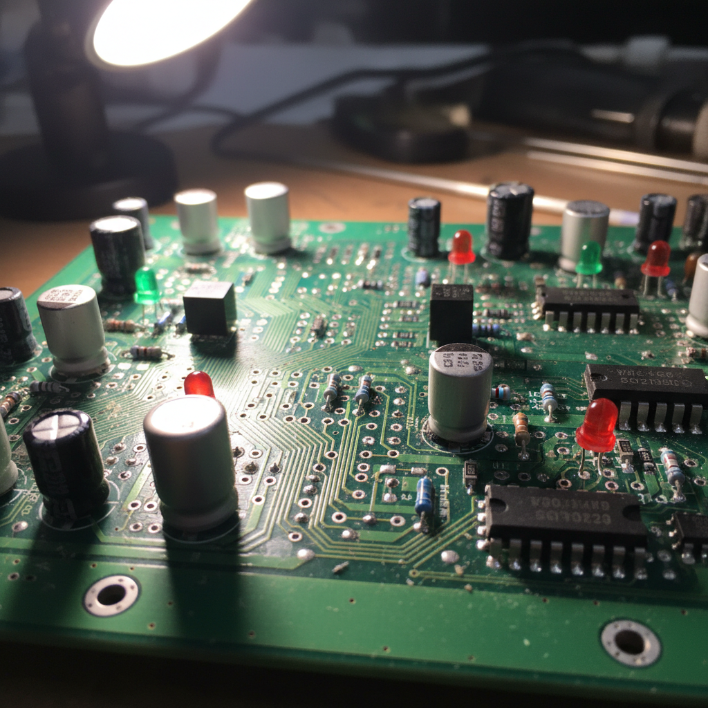
Every part on your BOM. Authenticated. In stock.
We pull from 14 authorized distributors simultaneously. Hard-to-find parts, last-time-buy components, and allocation-constrained ICs sourced through vetted broker networks with full authentication screening.
- ▸Parallel BOM fulfillment across Digi-Key, Mouser, Arrow, Avnet, and 10 additional authorized sources
- ▸Hard-to-find and EOL component sourcing through ERAI-registered brokers
- ▸Physical and electrical counterfeit screening on all broker-sourced components
- ▸Country-of-origin documentation available for ITAR/EAR compliance
- ▸Excess component storage and kitting for multi-revision builds
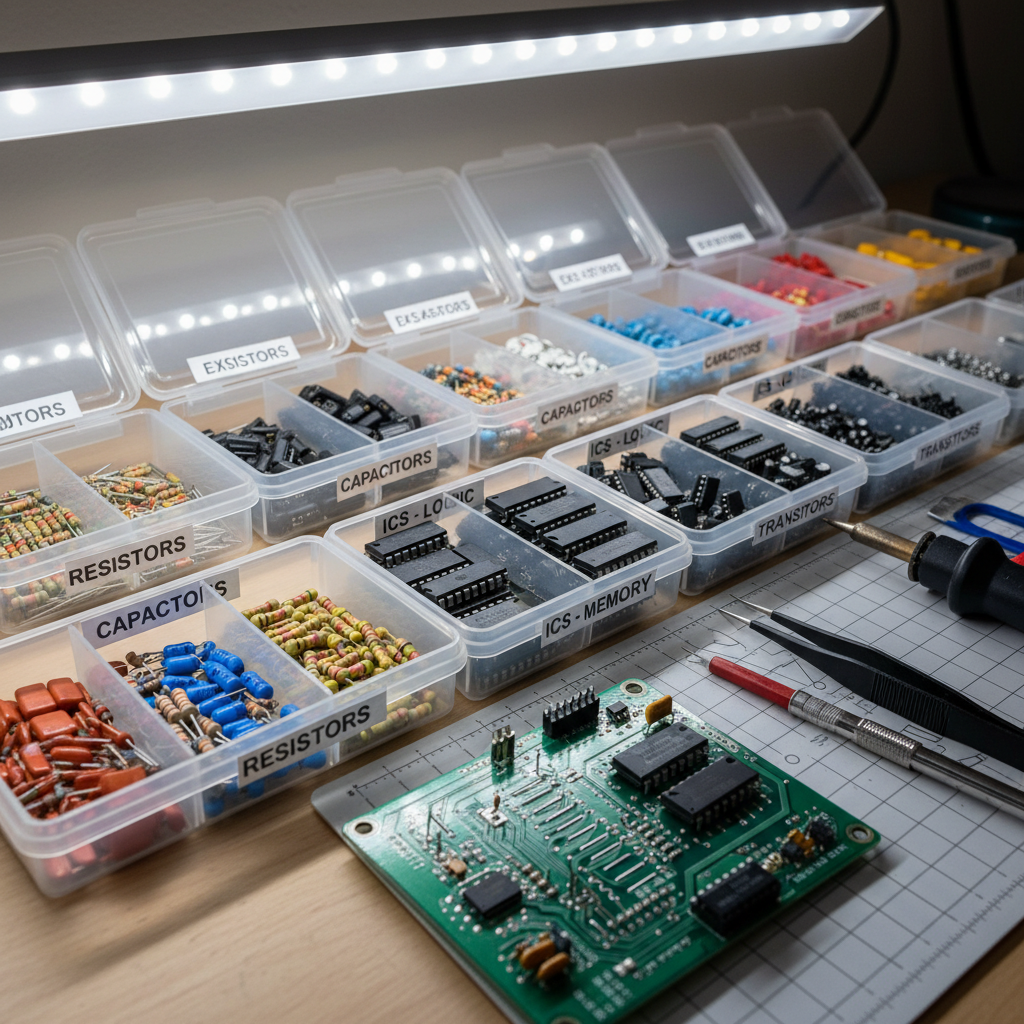
SMD down to 0201. THT hand-soldered. Same day.
Stencil-print, pick-and-place, reflow, wave solder, and hand-solder in a single shift. We run mixed-technology assemblies — SMD on both sides, through-hole on the back — without splitting into separate work orders.
- ▸DEK Horizon stencil printer with 3D SPI (solder paste inspection) on every board
- ▸Assembleon Emerald pick-and-place: 0201 standard, 01005 on request
- ▸Lead-free reflow with 8-zone profile; nitrogen atmosphere for fine-pitch BGA
- ▸X-ray inspection for BGA, QFN, and hidden solder joints
- ▸IPC-A-610 Class 2 workmanship inspection with photographic documentation
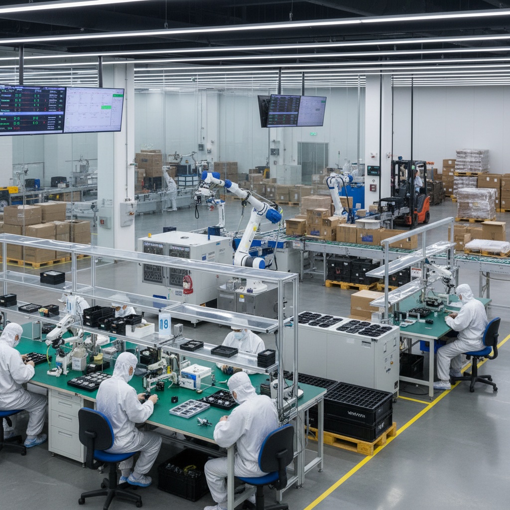
Every board leaves with a test report.
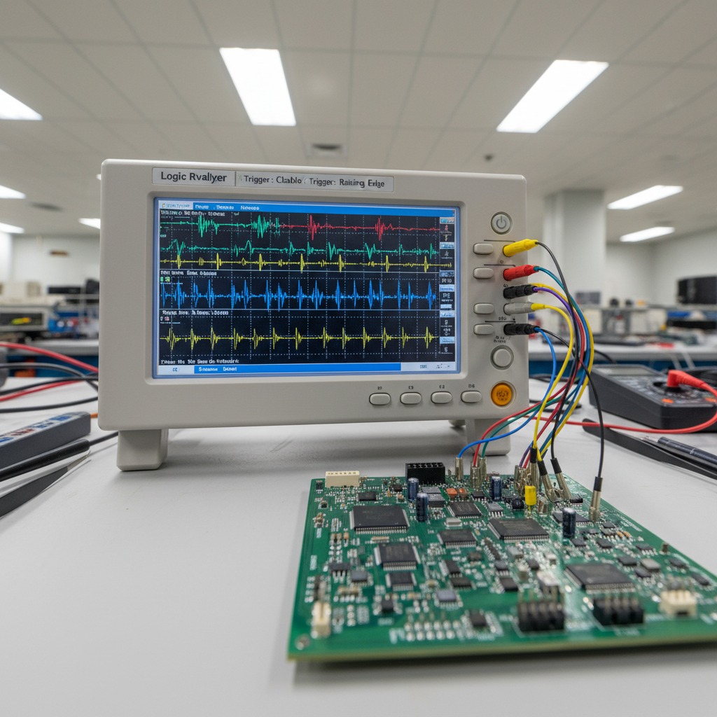
ICT, functional test, and boundary scan. We write the test fixture if you don't have one. Every board is electrically tested before it ships. No exceptions. Test reports are delivered with your boards.
- ▸In-circuit test (ICT) on bed-of-nails fixture: resistors, capacitors, diodes, ICs
- ▸Functional test fixtures built in-house — we write the test software to your specification
- ▸JTAG boundary scan for complex digital boards; SVF/XSVF programming support
- ▸Environmental stress screening (burn-in, thermal cycling) on request
- ▸Full photographic documentation of assembly and test at each stage
Every phase compressed. The traditional hardware development timeline assumes you have months. You don't. Every row below shows what we've eliminated.
Start Your Build
Upload your schematic or Gerber files. We'll respond with a detailed build quote — turnaround time, BOM cost, and first-pass yield estimate — within 4 business hours.
Start Your Build — Upload FilesAccepts: Gerber / KiCad / Eagle / Altium / PDF schematic · NDA available
Engineer-to-engineer.
No sales pitch.
What file formats do you accept?
How do you handle IP and design confidentiality?
What is your minimum trace width and via size?
Can you source components that are on allocation or obsolete?
What does "first-pass yield" mean for my project?
Do you support post-prototype production ramp?
Still have a specific technical question?
build@prototype.io
Built under pressure.
Delivered on deadline.
"We had 11 days to demo day. Prototype delivered a fully assembled 4-layer board with BLE and USB-C PD — tested, working, in my hand — with 3 days to spare. That's not a service, that's a co-founder."
"We needed 7 revision cycles compressed. Prototype ran three spins in parallel — different component footprints, different stackups — and we converged on a production-ready design in 9 days instead of 9 weeks."
"I promised 800 backers a working unit. Prototype took my KiCad files on Monday. By Thursday I was filming the unboxing video. The Kickstarter comment section went from 'scam' to 'legit' in 48 hours."